The entire semiconductor value chain (covering wafer manufacturing, thin film deposition, high-temperature crystal growth, equipment components, and advanced packaging) relies extremely on these two ultra-pure refractory metals, tungsten and molybdenum. With their extremely high melting points (3422°C for tungsten and 2622°C for molybdenum) and characteristics such as low impurity release, low thermal expansion, low resistivity, and low vapor pressure in a vacuum environment, the core products are classified into five categories. The following, based on real production cases from global leading wafer factories and major storage companies, provides a detailed analysis of the industry application and implementation results of each category of products.
1. Ultra-Pure Tungsten/Molybdenum Sputtering Targets
Product Description: The core products are 5N/6N ultra-pure molybdenum targets, tungsten targets, tungsten-titanium composite targets, and molybdenum alloy targets (sizes ranging from 8/12 inches), mainly used in PVD (Physical Vapor Deposition) processes for depositing metal films on silicon wafers. In traditional 28nm and above process technologies, tungsten targets dominated the filling of contact holes and gate barrier layers; while in 3nm/7nm advanced logic process and 300-layer or more 3D NAND, molybdenum targets are accelerating the replacement of tungsten targets. At the same line width, the resistivity of molybdenum is 40% lower than that of tungsten, and the high aspect ratio stacking does not require the use of TiN barrier layers, significantly improving the storage density.
Industry Implementation Cases:
SK Hynix 375-layer 3D NAND Production Line Upgrade: As the stack layer count exceeded 300, the original 286-layer tungsten word lines faced a sharp increase in resistance, excessive read/write latency, and the blocking layer occupying vertical space. Therefore, SK Hynix fully introduced 6N ultra-pure molybdenum target materials, equipped with dedicated ALD (Atomic Layer Deposition) furnaces, and eliminated the TiN blocking layer. A single batch could load 100 300mm wafers. After the upgrade, the chip unit area was reduced by 18%, the bit density increased by 16.3%; the contact resistance was reduced by 56%, and the read/write speed was increased by 22%. Reducing 15% of the deposition processes enabled a monthly cost savings of over 10 million RMB per factory. It is expected that by the end of 2026, its Cheongju factory will achieve full-scale production, with monthly molybdenum target procurement exceeding 2 tons.
Changan Storage Xtacking 3.0 Domestic Replacement: Changan Storage's 232-layer 3D NAND production line was previously highly dependent on Japanese Nishin Metal's molybdenum targets. Jin Mo Shares jointly with Longhua Technology successfully completed the domestic certification of 5N5 ultra-pure molybdenum target materials and supplied 12-inch target materials. The actual measurement showed that the impurity content of the domestic target materials was lower than 0.1 ppm, and the film uniformity was the same as the imported products, with a 32% reduction in single set equipment consumables cost. In 2025, both parties signed a 3-year long-term agreement, reducing import consumables expenditures by over 120 million RMB per year, achieving the independent control of the core coating materials for storage.
2. CVD Pre-Processing Gas
Product Description: The core product is high-purity molybdenum-based pre-processing gas, mainly used in CVD (Chemical Vapor Deposition) processes. Compared to PVD sputtering targets, pre-processing gas can achieve more excellent step coverage and more uniform film filling in the deposition of 3D NAND word lines with ultra-high aspect ratios (such as over 375 layers), being the core consumable supporting the implementation of ultra-high layer count NAND flash memory.
Industry Implementation Cases:
Global Storage Giants' 375-layer Production Line Process Upgrade: Facing the exponential increase in difficulty in trench etching and film deposition for ultra-high layer count 3D NAND, storage giants such as Samsung and SK Hynix in the 375-layer NAND production line upgrades fully equipped high-temperature molybdenum pre-processing gas supply systems. Due to the extremely high requirements for precursor gases in terms of impurity control and high-temperature vaporization formulations, leading suppliers such as Yaco Technology have successfully supplied to Samsung and SK Hynix with 6N grade molybdenum precursor technology, perfectly adapting to the new generation of NAND molybdenum word line CVD deposition process. The long-term demand has exploded in tandem with the production capacity of high-end NAND.
High-temperature molybdenum tungsten structural components (crystal growth and high-temperature heat treatment industry)
Product description: The core products include molybdenum crucibles, molybdenum material carts, molybdenum heat shields, TZM molybdenum support components, molybdenum heating belts, and tungsten heating elements, suitable for vacuum/hydrogen annealing at 1000–1800°C, blue sapphire crystal growth, and silicon carbide epitaxial furnaces, etc. under extreme conditions. Stainless steel and nickel-based alloys are prone to creep deformation and oxidation cracking above 1000°C, while molybdenum/tungsten does not oxidize or release impurities in an inert atmosphere, and the creep resistance of TZM molybdenum is twice that of pure molybdenum, effectively avoiding wafer metal contamination.
Industry implementation cases:
Upgrade of Mini LED blue sapphire growth furnace at Sanan Optoelectronics: Sanan Optoelectronics originally used imported molybdenum crucibles for blue sapphire growth, with a lifespan of only 90 days. Frequent furnace shutdowns severely restricted production capacity. By using thin-walled molybdenum crucibles made from high-purity Mo-1 molybdenum ingots and polishing the inner walls to a mirror surface level, the continuous lifespan of a single crucible increased to 280 days (3 times improvement), the growth yield increased from 82% to 91%, and the annual substrate production per furnace increased by 120,000 pieces. After 200 growth furnaces nationwide were fully replaced with domestic crucibles, annual equipment and material cost savings exceeded 60 million RMB.
IV. Tungsten copper/molybdenum copper composite heat sinks (advanced packaging and power device industry)
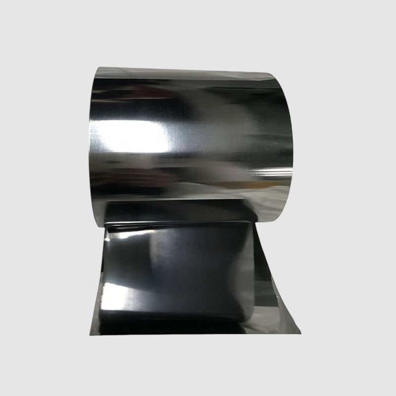
Product description: The core products are WCu70/80 tungsten copper, MoCu molybdenum copper heat sink substrates, and tungsten copper substrates, mainly used for the packaging of GPUs, HBM (high-bandwidth memory), IGBT, and power semiconductors. The process adaptation lies in: the low thermal expansion coefficients of tungsten and molybdenum perfectly match silicon and gallium nitride chips, while the high thermal conductivity of copper can quickly conduct heat. This composite material effectively solves the problem of AI large computing power chips' frequency reduction and thermal failure under high temperatures, becoming an ideal substitute for pure copper and aluminum substrates.
Industry implementation case:
Upgrade of thermal management for AI large computing power chips: With the surge in computing power requirements for AI large models on GPUs and HBM chips, the heat flux density has reached its limit. Traditional pure copper substrates, due to their mismatched thermal expansion coefficients, are prone to weld fatigue failure under long-term high-temperature cycling. Using MoCu molybdenum copper composite heat sink substrates not only achieves perfect thermal expansion matching with silicon chips but also significantly reduces the thermal resistance, completely solving the thermal failure problem of AI chips under high-frequency operation, ensuring the long-term stable operation of computing infrastructure.
V. Precision tungsten molybdenum alloy components (semiconductor equipment component industry)
Product description: The core products are precision tungsten molybdenum components for semiconductor equipment, such as ion implantation machine shielding components, MOCVD heaters, and electronic packaging heat sinks materials. These components need to maintain extremely high dimensional accuracy and physical stability in extremely high vacuum and corrosive environments, being the "invisible cornerstone" for semiconductor equipment to achieve precise processes.
Industry implementation case:
Domesticization of core components of semiconductor ion implantation machines: In response to the pain point of long-term reliance on imports for high-end tungsten molybdenum components for 3.5-generation semiconductor ion implantation machines, domestic enterprises such as Xingyao Xincai have successfully developed and produced precision tungsten molybdenum components with a purity of over 99.99%. These components exhibit extremely long lifespans and stable performance under long-term high-vacuum ion bombardment, successfully entering the supply chains of domestic and foreign customers, breaking the monopoly of overseas companies, and achieving domestic substitution for key components of semiconductor equipment.

 EN
EN

 Hot News